Advanced compact model and processing circuit for integrated magnetic sensor systems
Abstract: The generalized electric model of the Hall sensor, which is designed
for circuit simulation, is taken into account the features of its design and used for
manufacturing materials. The model of the Hall sensor is implemented in the
language Verilog-A, has a simple structure and allows to accurately describe its
performance characteristics. The equivalent circuit of the sensor is built on the
basis of standard subcomponents and does not use complex equations to describe
the physical processes in its structure. A circuit and topological solution consisting
of Hall sensor, differential amplifier and 10-bit successive approximation register
analog-to-digital converter and other components integrated on a single chip using
the TSMC 0.18 μm CMOS MS/RF 1,8/3,3V PDK design library, allowing to receive
and process data of sensor devices.
Trang 1
Trang 2
Trang 3
Trang 4
Trang 5
Trang 6
Trang 7
Trang 8
Tóm tắt nội dung tài liệu: Advanced compact model and processing circuit for integrated magnetic sensor systems
Kỹ thuật điện tử
D. D. Ha, T. T. Trung, “Advanced compact model  integrated magnetic sensor systems.” 196
ADVANCED COMPACT MODEL AND PROCESSING CIRCUIT
FOR INTEGRATED MAGNETIC SENSOR SYSTEMS
Dao Dinh Ha
1*
, Tran Tuan Trung
2
Abstract: The generalized electric model of the Hall sensor, which is designed
for circuit simulation, is taken into account the features of its design and used for
manufacturing materials. The model of the Hall sensor is implemented in the
language Verilog-A, has a simple structure and allows to accurately describe its
performance characteristics. The equivalent circuit of the sensor is built on the
basis of standard subcomponents and does not use complex equations to describe
the physical processes in its structure. A circuit and topological solution consisting
of Hall sensor, differential amplifier and 10-bit successive approximation register
analog-to-digital converter and other components integrated on a single chip using
the TSMC 0.18 μm CMOS MS/RF 1,8/3,3V PDK design library, allowing to receive
and process data of sensor devices.
Keywords: Hall sensor; Compact Model; Verilog-A; Signal processing circuit; Analog-to-digital converter.
1. INTRODUCTION
In modern electronics sensors for measuring the induction of a magnetic field,
contactless determination of mechanical and electrical influences is widely used.
This type of sensor is used in the automotive, mobile and consumer segments,
medicine, aerospace and marine industries, power engineering – as sensors for
cameras and displays, electronic compasses, etc. [1]. For practical applications, the
Hall sensor (HS) is usually placed with a signal processing circuit on a single chip.
However, the constructive implementation of such a system remains a problem,
because the sensor models are not included in the design library provided by the
chip manufacturer. Standard models for describing the electrical characteristics of
HS are too complex [2] or idealized [3]. 2D or 3D physical models described by
FEM simulators for integration with circuit simulation programs require significant
computational costs [3], but are useful for analyzing the effect of geometric
parameters on the behavior of a sensor. To improve design efficiency and system
performance, it is necessary to have an electrical (SPICE) model that adequately
describes the characteristics of the sensor element. Such a model describes the
behavior of the sensor using a set of equations obtained by means of adequate
assumptions and simplifications.
Another important task in the field of sensor design is the development of
systems that provide accurate processing of input data, as well as their conversion
to a digital signal. The latter would greatly simplify the process of further analysis
of the results of measurements. These tasks can be solved by sharing amplifiers
and analog-to-digital converters, which enable the transition to a digital
representation of the original analog signal with small amplitude.
The paper presents the results of the development of a unified compact model of
a Hall sensor fabricated both by standard silicon technology and based on wide-
gap semiconductors. The model also provides the ability to account for the
material and geometry of the integrated magnetic concentrator (IMC) designed to
increase the sensitivity of the sensor. A circuit-based solution consisting of a low-
Nghiên cứu khoa học công nghệ
Tạp chí Nghiên cứu KH&CN quân sự, Số Đặc san Viện Điện tử, 9 - 2020 197
noise amplifier and an analog-to-digital converter, which allows receiving and
processing of sensor data, is developed and topologically realized.
2. SIMULATION TOOLS, INVESTIGATED SENSOR CONSTRUCTIONS
AND COMPACT MODEL DESCRIPTION
2.1. Investigated Hall Sensor designs
In the calculations presented below, the simulation of the electric characteristics
of the Hall sensor was carried out in the Silvaco software environment [4], the
IMC parameters were calculated in the FEMM program [5], the Verilog-A [6]
language was used to develop the electrical model, and the compact model and
circuit solutions were designed and tested using Cadence software [7].
Fig. 1 shows the HS designs that are being investigated. The design presented
on the left is a sensor manufactured using standard silicon technology [8], the
design on the right is a sensor based on gallium nitride [9].
L
W
Sapphire (0001)
contact
AlxGa1-xN
GaN
AlN
Ti/Al/Ni/Au
L
W
n-well
depletion layer
p-substrate
contact
n+ n+
oxide
t
Figure 1. Investigated Hall Sensors designs.
1
2
2
3
θ
l
d
D
4
Figure 2. Modeling determining the parameters of material sample by CST.
Kỹ thuật điện tử
D. D. Ha, T. T. Trung, “Advanced compact model  integrated magnetic sensor systems.” 198
Fig. 2 shows the sensor system design, which includes an IMC. It consists of
four HS (2) and an IMC (3) formed on a silicon substrate (1). Four HS are
perpendicular to each other along the edges of the IMC. Between the IMC and the
HS there is a dielectric layer (4) of thickness d. The IMC is a disk of a
ferromagnetic material with a diameter D, a thickness l, and a deflection angle θ.
Supermindur which has a high induction of magnetic saturation was used as the
IMC material. Earlier studies were carried out to optimize the design and
technology, electrical and operational characteristics of presented sensors types
within the device-technological simulation [8-10, 12].
2.2. Advanced compact model of the Hall Sensor
Fig. 3 shows an equivalent circuit describing the HS compact. For an ideal
design (no technological discrepancy and mechanical stress in the system), the van
der Pauw method is used to measure the surface resistance of the RS layer. Since
the device is symmetrical, it is necessary to determine the values of the two
resistances between the contacts: RD for the resistance between the two opposite
and RH for the two adjacent contacts [11]. In comparison with the existing
solutions [12], this scheme provides the possibility of taking into account the
galvanomagnetic and temperature effects.
INPUT
CCVS1
CCVS4
CCVS3
CCVS2
RH RD
-
+
- +
-
+
-+
INPUT
OUTPUTOUTPUT
RD RD
RD
RH RH
RH
2
1
4
3
5
B
R
Figure 3. Equivalent circuit describing the basic HS compact model.
The proposed equivalent circuit has 4 electrical outputs and one external source
as input (B) and includes the following components: 8 non-linear resistors
designed to describe the dependences of the characteristics of the HS from the
magnetic field and temperature; 4 current-controlled voltage sources, which allow
estimating the contributions to the Hall voltage of currents flowing through
nonlinear resistances; 4 interface blocks for the simulation of series resistances.
The parameters of the silicon-based HS compact model [11] are given in Table 1.
Nghiên cứu khoa học công nghệ
Tạp chí Nghiên cứu KH&CN quân sự, Số Đặc san Viện Điện tử, 9 - 2020 199
The last two lines contain the parameters typical for the hall sensor made on the
basis of wide-gap semiconductors. The names of electrical model parameters used
in the text are shown in parentheses. To simulate the magnetosensitive sensor with
IMC, added the parameters presented in Table 2.
Table 1. Silicon based hall sensor model parameters.
Parameter Description Unit Value range
TEMP Ambient temperature K 248–398
L Length of active area m (30–120)×10-6
W Active Area Width m (10–40)×10-6
S (s) Size of the contact electrode M (9–39)×10-6
TETA (θ) Hall angle radians 0–0.45
RH (rH) The Hall Scattering Coefficient 0.2–1.7
GH (GH) Correction geometric coefficient 0,5–1
NDNW (ND,NW)
Concentration of charge carriers in
the active region
m
-3
 10
21–1023
NSUB (NSUB)
Concentration of charge carriers in a
substrate
m
-3
 5×10
20–1021
DEFF (deff) Effective depth of active area m (0.5–5)×10
-6
MOBN (µn)
Mobility of electrons in the active
region
m
2/V∙s 0.072–0.141
MOBH (µh)
Mobility of holes in the active
region
m
2/V∙s 0.032–0.047
RSS (RS) Surface resistance of silicon Ohm 100–15×10
3
RDD (RD)
Resistance between two opposite
contacts
Ohm 650–120×103
RHH (RH)
Resistance between two neighboring
opposites
Ohm 1100–200×103
BBR1
The first coefficient of resistance
versus voltage
V
-1
 0–0.01
BBR2
The second coefficient of resistance
versus voltage
V
-2
 -0.005–0
BBS1
The first coefficient of sensitivity
versus voltage
V
-1
 0–0.01
BBS2
The second coefficient of sensitivity
versus voltage
V
-2
 -0.005–0
RTC1
The first temperature coefficient of
resistance
V
-1
 0–0.01
RTC2
The second temperature coefficient
of resistance
V
-2
 0–0.0005
ALPHA (αSI)
Temperature coefficient of
sensitivity
V
-1
 0–0.001
NSS (NS)
Concentration of charge carriers in
2DEG
m
-2
 10
16–1018
MOBN (µS) Mobility of electrons in 2DEG m
2/V∙s 0.01–1.0
Kỹ thuật điện tử
D. D. Ha, T. T. Trung, “Advanced compact model  integrated magnetic sensor systems.” 200
Table 2. The compact model parameters of the magnetosensitive sensor with IMC.
Parameter Description Unit Value range
D Diameter of the concentrator m (50–500)×10-6
t Thickness of concentrator m (5–20)×10-6
Mu0 (µ0) Magnetic permeability (1–100)×10
3
BSAT (Bsat) Magnetic saturation induction Tesla 1–2.8
N Demagnetization factor 0.015–0.15
K Coefficient of magnetic flux 5–20
3. SIMULATION RESULTS
3.1. Device-technological vs. Schematic simulation
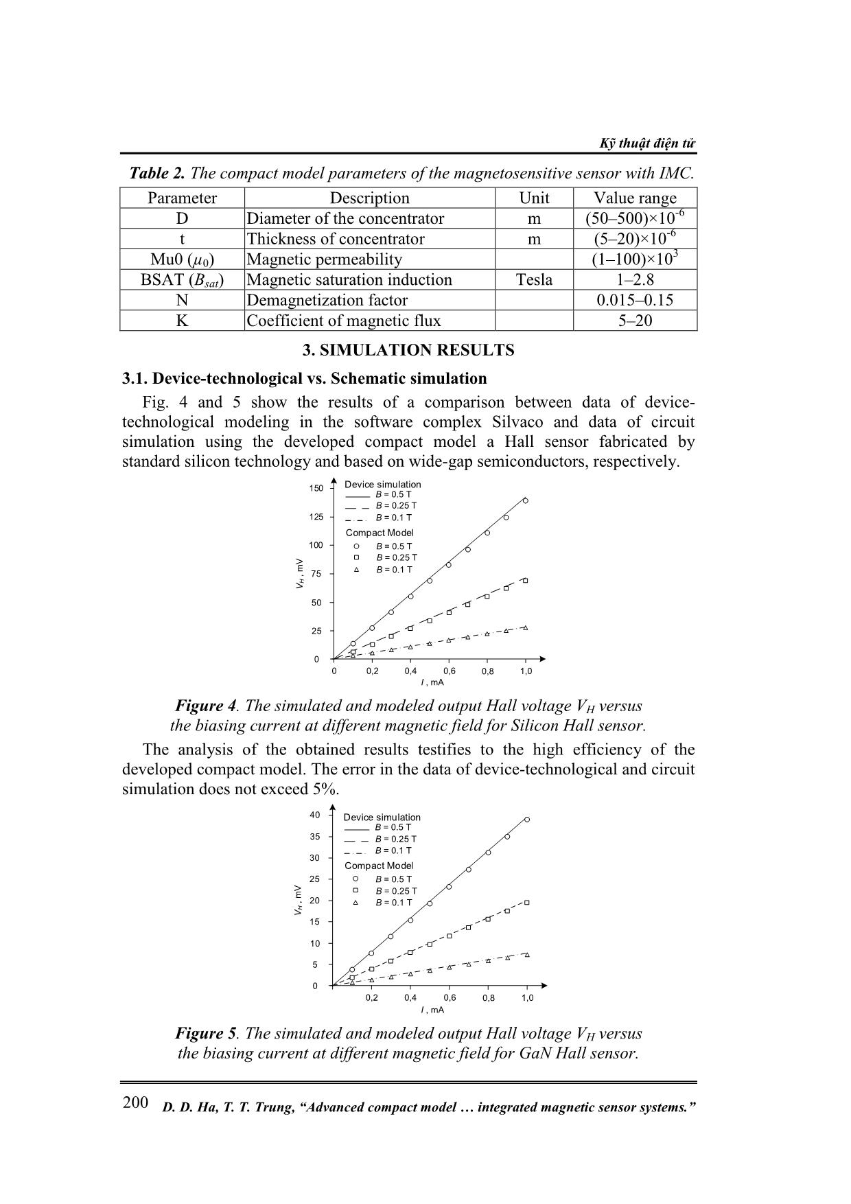
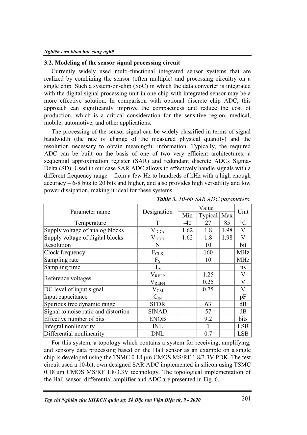
Fig. 4 and 5 show the results of a comparison between data of device-
technological modeling in the software complex Silvaco and data of circuit
simulation using the developed compact model a Hall sensor fabricated by
standard silicon technology and based on wide-gap semiconductors, respectively.
0 0,2 0,4 0,6 0,8 1,0
150
125
100
75
50
25
0
I , mA
V
H
 ,
 m
V
Device simulation
B = 0.25 T
B = 0.1 T
B = 0.5 T
Compact Model
B = 0.25 T
B = 0.1 T
B = 0.5 T
Figure 4. The simulated and modeled output Hall voltage VH versus
the biasing current at different magnetic field for Silicon Hall sensor.
The analysis of the obtained results testifies to the high efficiency of the
developed compact model. The error in the data of device-technological and circuit
simulation does not exceed 5%.
0,2 0,4 0,6 0,8 1,0
40
35
30
25
10
5
0
I , mA
V
H
 ,
 m
V
20
Device simulation
B = 0.1 T
B = 0.5 T
Compact Model
B = 0.1 T
B = 0.5 T
B = 0.25 T
B = 0.25 T
15
Figure 5. The simulated and modeled output Hall voltage VH versus
the biasing current at different magnetic field for GaN Hall sensor.
Nghiên cứu khoa học công nghệ
Tạp chí Nghiên cứu KH&CN quân sự, Số Đặc san Viện Điện tử, 9 - 2020 201
3.2. Modeling of the sensor signal processing circuit
Currently widely used multi-functional integrated sensor systems that are
realized by combining the sensor (often multiple) and processing circuitry on a
single chip. Such a system-on-chip (SoC) in which the data converter is integrated
with the digital signal processing unit in one chip with integrated sensor may be a
more effective solution. In comparison with optional discrete chip ADC, this
approach can significantly improve the compactness and reduce the cost of
production, which is a critical consideration for the sensitive region, medical,
mobile, automotive, and other applications.
The processing of the sensor signal can be widely classified in terms of signal
bandwidth (the rate of change of the measured physical quantity) and the
resolution necessary to obtain meaningful information. Typically, the required
ADC can be built on the basis of one of two very efficient architectures: a
sequential approximation register (SAR) and redundant discrete ADCs Sigma-
Delta (SD). Used in our case SAR ADC allows to effectively handle signals with a
different frequency range – from a few Hz to hundreds of kHz with a high enough
accuracy – 6-8 bits to 20 bits and higher, and also provides high versatility and low
power dissipation, making it ideal for these systems.
Table 3. 10-bit SAR ADC parameters.
Parameter name Designation
Value
Unit
Min Typical Max
Temperature T -40 27 85 °C
Supply voltage of analog blocks VDDA 1.62 1.8 1.98 V
Supply voltage of digital blocks VDDD 1.62 1.8 1.98 V
Resolution N 10 bit
Clock frequency FCLK 160 MHz
Sampling rate FS 10 MHz
Sampling time TS ns
Reference voltages
VREFP 1.25 V
VREFN 0.25 V
DC level of input signal VCM 0.75 V
Input capacitance CIN pF
Spurious free dynamic range SFDR 63 dB
Signal to noise ratio and distortion SINAD 57 dB
Effective number of bits ENOB 9.2 bits
Integral nonlinearity INL 1 LSB
Differential nonlinearity DNL 0.7 LSB
For this system, a topology which contains a system for receiving, amplifying,
and sensory data processing based on the Hall sensor as an example on a single
chip is developed using the TSMC 0.18 μm CMOS MS/RF 1.8/3.3V PDK. The test
circuit used a 10-bit, own designed SAR ADC implemented in silicon using TSMC
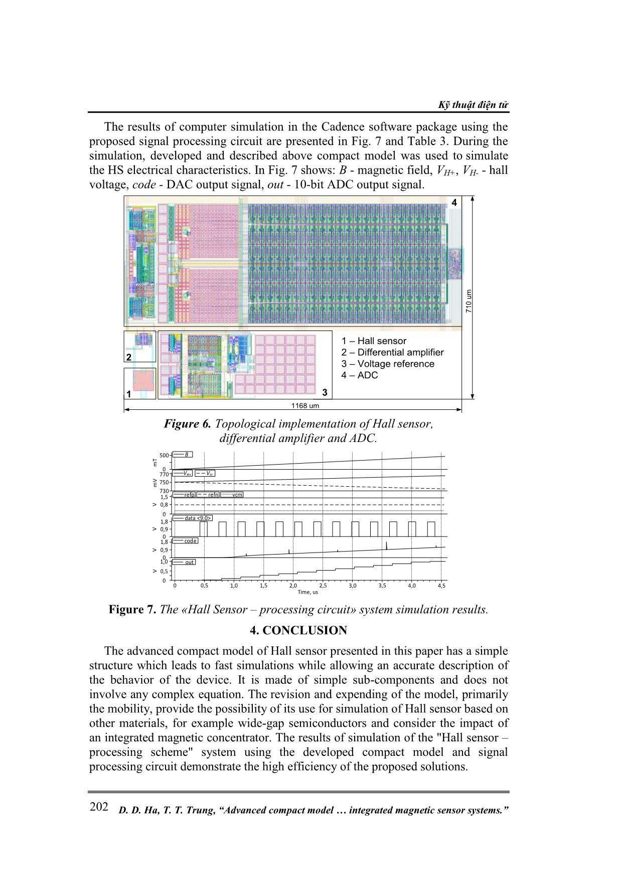
0.18 um CMOS MS/RF 1.8/3.3V technology. The topological implementation of
the Hall sensor, differential amplifier and ADC are presented in Fig. 6.
Kỹ thuật điện tử
D. D. Ha, T. T. Trung, “Advanced compact model  integrated magnetic sensor systems.” 202
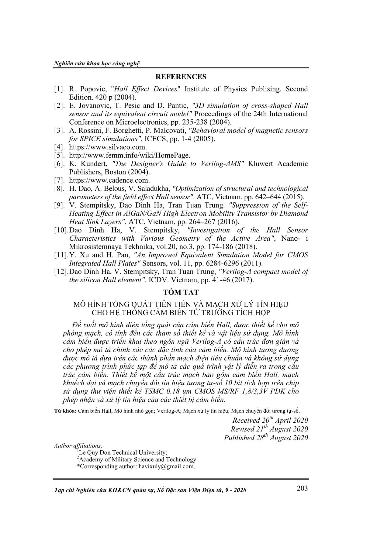
The results of computer simulation in the Cadence software package using the
proposed signal processing circuit are presented in Fig. 7 and Table 3. During the
simulation, developed and described above compact model was used to simulate
the HS electrical characteristics. In Fig. 7 shows: B - magnetic field, VH+, VH- - hall
voltage, code - DAC output signal, out - 10-bit ADC output signal.
1 – Hall sensor
2 – Differential amplifier
3 – Voltage reference
4 – ADC
4
31
2
1168 um
7
1
0
 u
m
Figure 6. Topological implementation of Hall sensor,
differential amplifier and ADC.
0
500
0
В
m
T
1,8
0,9V
730
770
750
VH+ VH-
m
V
0
1,5
0,8
refp refn vcm
V
data
1,8
0
0,9
code
V
0,5
0
out
V
1,00,50 2,01,5 3,02,5 4,03,5 4,5
1,0
Time, us
Figure 7. The «Hall Sensor – processing circuit» system simulation results.
4. CONCLUSION
The advanced compact model of Hall sensor presented in this paper has a simple
structure which leads to fast simulations while allowing an accurate description of
the behavior of the device. It is made of simple sub-components and does not
involve any complex equation. The revision and expending of the model, primarily
the mobility, provide the possibility of its use for simulation of Hall sensor based on
other materials, for example wide-gap semiconductors and consider the impact of
an integrated magnetic concentrator. The results of simulation of the "Hall sensor –
processing scheme" system using the developed compact model and signal
processing circuit demonstrate the high efficiency of the proposed solutions.
Nghiên cứu khoa học công nghệ
Tạp chí Nghiên cứu KH&CN quân sự, Số Đặc san Viện Điện tử, 9 - 2020 203
REFERENCES
[1]. R. Popovic, "Hall Effect Devices" Institute of Physics Publising. Second
Edition. 420 p (2004).
[2]. E. Jovanovic, T. Pesic and D. Pantic, "3D simulation of cross-shaped Hall
sensor and its equivalent circuit model" Proceedings of the 24th International
Conference on Microelectronics, pp. 235-238 (2004).
[3]. A. Rossini, F. Borghetti, P. Malcovati, "Behavioral model of magnetic sensors
for SPICE simulations", ICECS, pp. 1-4 (2005).
[4]. https://www.silvaco.com.
[5].
[6]. K. Kundert, "The Designer's Guide to Verilog-AMS" Kluwert Academic
Publishers, Boston (2004).
[7]. https://www.cadence.com.
[8]. H. Dao, A. Belous, V. Saladukha, "Optimization of structural and technological
parameters of the field effect Hall sensor". ATC, Vietnam, pp. 642–644 (2015).
[9]. V. Stempitsky, Dao Dinh Ha, Tran Tuan Trung. "Suppression of the Self-
Heating Effect in AlGaN/GaN High Electron Mobility Transistor by Diamond
Heat Sink Layers". ATC, Vietnam, pp. 264–267 (2016).
[10]. Dao Dinh Ha, V. Stempitsky, "Investigation of the Hall Sensor
Characteristics with Various Geometry of the Active Area", Nano- i
Mikrosistemnaya Tekhnika, vol.20, no.3, pp. 174-186 (2018).
[11]. Y. Xu and H. Pan, "An Improved Equivalent Simulation Model for CMOS
Integrated Hall Plates" Sensors, vol. 11, pp. 6284-6296 (2011).
[12]. Dao Dinh Ha, V. Stempitsky, Tran Tuan Trung, "Verilog-A compact model of
the silicon Hall element". ICDV. Vietnam, pp. 41-46 (2017).
TÓM TẮT
MÔ HÌNH TỔNG QUÁT TIÊN TIẾN VÀ MẠCH XỬ LÝ TÍN HIỆU
CHO HỆ THỐNG CẢM BIẾN TỪ TRƯỜNG TÍCH HỢP
Đề xuất mô hình điện tổng quát của cảm biến Hall, được thiết kế cho mô
phỏng mạch, có tính đến các tham số thiết kế và vật liệu sử dụng. Mô hình
cảm biến được triển khai theo ngôn ngữ Verilog-A có cấu trúc đơn giản và
cho phép mô tả chính xác các đặc tính của cảm biến. Mô hình tương đương
được mô tả dựa trên các thành phần mạch điện tiêu chuẩn và không sử dụng
các phương trình phức tạp để mô tả các quá trình vật lý diễn ra trong cấu
trúc cảm biến. Thiết kế một cấu trúc mạch bao gồm cảm biến Hall, mạch
khuếch đại và mạch chuyển đổi tín hiệu tương tự-số 10 bit tích hợp trên chip
sử dụng thư viện thiết kế TSMC 0.18 um CMOS MS/RF 1,8/3,3V PDK cho
phép nhận và xử lý tín hiệu của các thiết bị cảm biến.
Từ khóa: Cảm biến Hall, Mô hình nhỏ gọn; Verilog-A; Mạch xử lý tín hiệu; Mạch chuyển đổi tương tự-số.
Received 20
th
 April 2020
Revised 21
th
 August 2020
Published 28
th
 August 2020
Author affiliations:
1
Le Quy Don Technical University;
2
Academy of Military Science and Technology.
*Corresponding author: havixuly@gmail.com.
File đính kèm:
 advanced_compact_model_and_processing_circuit_for_integrated.pdf

