Fabrication of a normally - On organic thin film transistor for active sensor construction
In organic active pressure sensor, a reduction in supply voltage of transistor is an effective
way to decrease the power consumption. Up to now, for the development of pressure sensor
based on normally-on OTFT (organic thin-film transistor), the OTFT where the conductive
channel is formed without gate voltage supply, is still challenging. In this paper, we
propose an approach to fabricate normally-on OTFT based on floating gate, photoactive
gate dielectric layer and programming process using external UV source. After fabrication,
measurements of OTFT characteristics, including transfer and output, were performed.
Estimation of the critical parameters including the threshold voltage and field effect
mobility was also described. Our fabricated OTFT shows good performance with a low
threshold voltage of -4 V and high mobility of 0.893 cm2/Vs. Before programming, the OTFT
is at normally-off state with drain current of 10-13 A at 0 V gate voltage. After programming,
the OTFT changes to normally-on state with drain current of 10-6 A at 0 V gate voltage.
OTFT fabrication is the essential step to construct an organic active pressure sensor in the
future work.
Trang 1
Trang 2
Trang 3
Trang 4
Trang 5
Trang 6
Trang 7
Trang 8
Trang 9
Trang 10
Tóm tắt nội dung tài liệu: Fabrication of a normally - On organic thin film transistor for active sensor construction
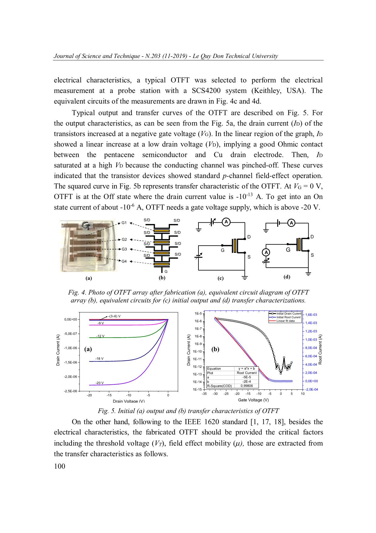
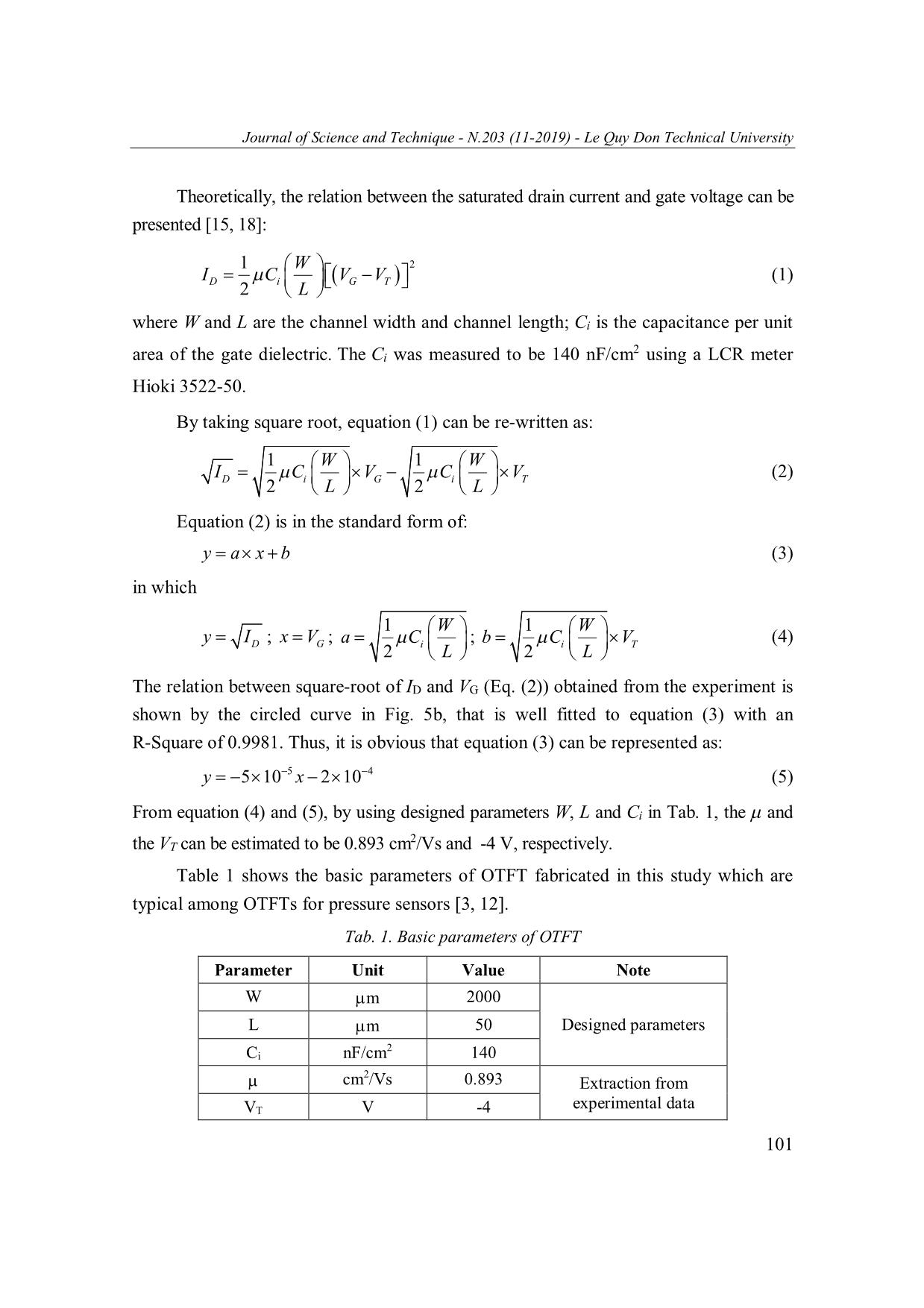
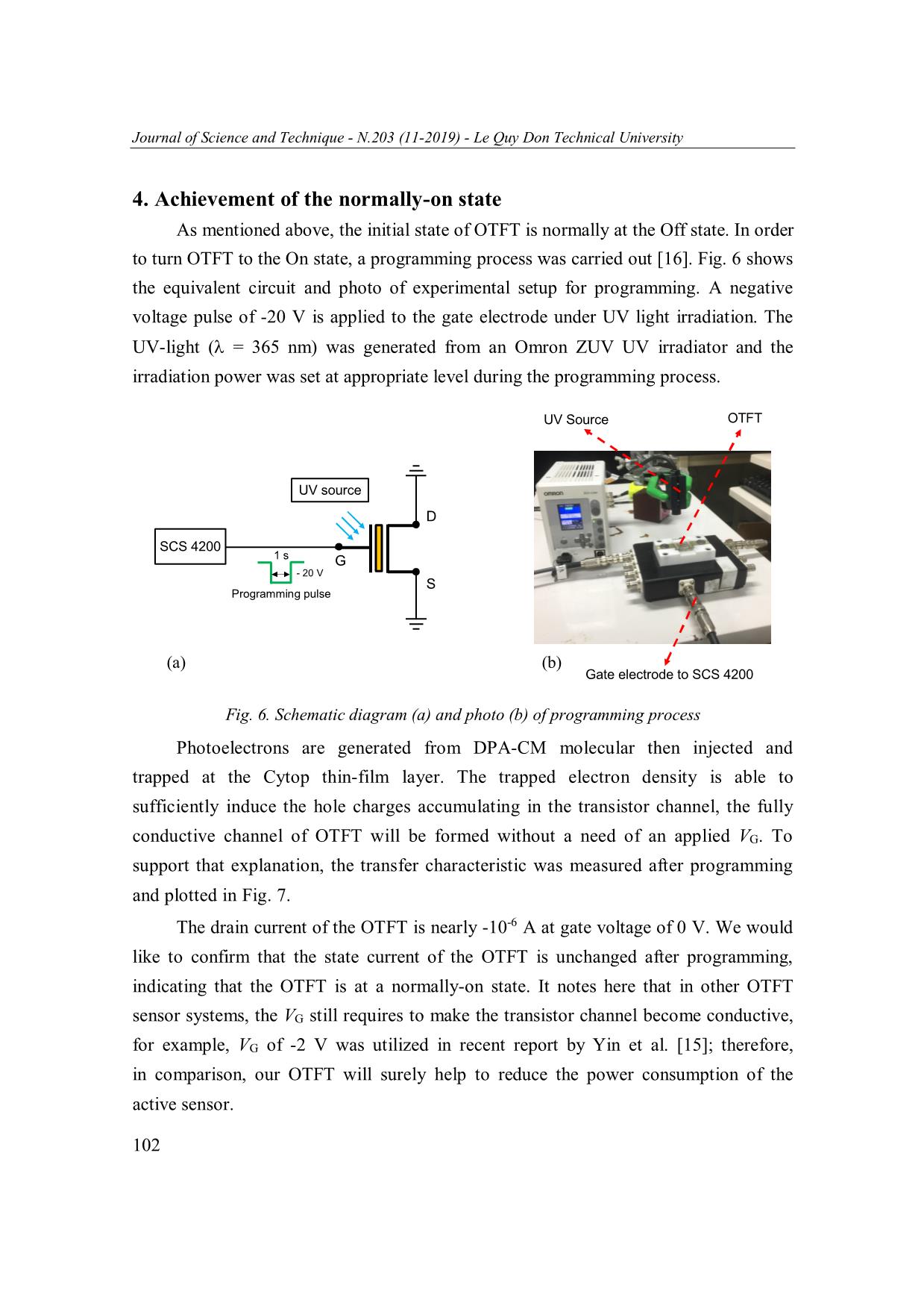
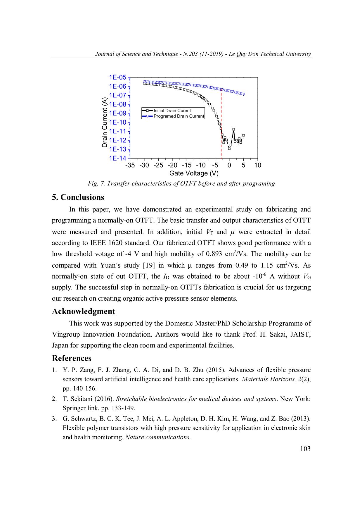
Journal of Science and Technique - N.203 (11-2019) - Le Quy Don Technical University FABRICATION OF A NORMALLY-ON ORGANIC THIN FILM TRANSISTOR FOR ACTIVE SENSOR CONSTRUCTION Khong Duc Chien1,2*, Hoang Van Phuc1, Dao Thanh Toan2 1Le Quy Don Technical University; 2University of Transport and Communications Abstract In organic active pressure sensor, a reduction in supply voltage of transistor is an effective way to decrease the power consumption. Up to now, for the development of pressure sensor based on normally-on OTFT (organic thin-film transistor), the OTFT where the conductive channel is formed without gate voltage supply, is still challenging. In this paper, we propose an approach to fabricate normally-on OTFT based on floating gate, photoactive gate dielectric layer and programming process using external UV source. After fabrication, measurements of OTFT characteristics, including transfer and output, were performed. Estimation of the critical parameters including the threshold voltage and field effect mobility was also described. Our fabricated OTFT shows good performance with a low threshold voltage of -4 V and high mobility of 0.893 cm2/Vs. Before programming, the OTFT is at normally-off state with drain current of 10-13 A at 0 V gate voltage. After programming, the OTFT changes to normally-on state with drain current of 10-6 A at 0 V gate voltage. OTFT fabrication is the essential step to construct an organic active pressure sensor in the future work. Keywords: Organic thin-film transistor; OTFT fabrication; normally on OTFT; organic active pressure sensor. 1. Introduction In recent years, a pressure sensor using organic material has attracted a lot of interest from many researchers due to its unique advantages including low temperature processing, solution process ability, low manufacturing cost, mechanical flexibility, and large-area possibility [1-12]. In terms of structure, an organic active pressure sensor device consists of passive element integrating with organic thin-film transistor [1-4]. In a standard active sensor cell, the passive device has been designed and fabricated in connection to the input gate electrode (G) of transistor as illustrated in Fig. 1 [1-4]. However, organic semiconductor basically does not have available carriers, thus if a voltage (VG) is not applied to the gate electrode, the conductive channel in the semiconductor layer is not formed, as presented in Fig. 1a (so-called normally-off state). To turn the transistor element of active sensor conductive, a certain value of VG needs to * Email: kchien.tdc@gmail.com 96 Journal of Science and Technique - N.203 (11-2019) - Le Quy Don Technical University be provided to create an electric field, which will induce the accumulated carriers from the source electrode (S) into the semiconducting channel as described in Fig. 1a. Even the sensing signal is amplified, sensor power consumption is large because both the drain voltage (VD) and the VG are used during sensor operating [3, 4]. VG VD VD Passive D Passive D pressure pressure sensor sensor G S G S (a) (b) Fig. 1. Active sensor structure using (a) normally-off and (b) normally-on OTFT. At device level, it is figured out that reduction of the supply voltage is the most effective way to scale down the power consumption [1, 2]. It is clear that VD is the essential voltage to create ID by collecting the induced carriers in the semiconductor layer. Consequently, the VG should be the objective to study for decreasing the sensor power consumption. Following that idea, in some active research groups, to construct an active sensor device, the second gate electrode of metal or electrolyte has been inserted into OTFT (called floating-gate) and directly connected to the output electrode of passive element as shown in Fig. 1b [14-16]. That allows the electricity from passive element directly charge the floating-gate, resulting in the enhancement of the accumulated carriers in the semiconductor layer due to built-in potential by the floating- gate. The VG could be significantly decreased, but a certain value was still required to make the transistor channel become conductive during sensor operating, for example, VG of -2 V was utilized in recent report by Yin et al. [15]. In this paper, we present a process where a normally-on OTFT using a Cytop floating-gate is fabricated. Firstly, fabrication process is presented in detail, then, the basic parameters are obtained following the IEEE 1640 standard. Finally, programming operation of the transistor is performed. The injected electrons are trapped and released at the Cytop floating-gate layer under external programming voltage. The trapped electron density is able to sufficiently induce the hole charges accumulating in the transistor channel, the fully conductive channel of OTFT will ... ubstrates coated with a 150 nm gate electrode layer of indium tin oxide (ITO) were cleaned in acetone and isopropanol in sequence for 10 min each using ultrasonication, followed by UV-O3 treatment. For the second step, photoactive molecules of DPA-CM and PMMA (Aldrich, USA, Mw = 94,600) were dissolved in a chloroform at a 1:10 molar ratio of a monomer unit of PMMA (2 wt%) to DPA-CM. A gate dielectric layer of DPA- CM and PMMA was prepared by spin-coating of the solution on the ITO/glass substrate at 4000 rpm for 60 s, and heated on a hot plate at 100C for 60 min to remove residual solvent. For the third step, the CYTOP layer (CTX-809AP2, Asahi Glass, Japan) was spin-coated onto the DPA-CM:PMMA gate dielectric layer at 2000 rpm for 60 s using a 0.5 wt% fluoro carbon solution and dried at 100C for 1 h. 98 Journal of Science and Technique - N.203 (11-2019) - Le Quy Don Technical University For the fourth step, dielectric DPA-CM:PMMA and Cytop layers were partly removed from the substrate at the position of the source and drain electrodes. For the fifth step, a 30-nm-thick film of pentacene was formed on the CYTOP layer by conventional vacuum deposition method at a deposition rate of 0.02 nm s-1. The vacuum deposition processes were performed at a pressure of 2×10⁻⁶ Torr. For the sixth step, the fabrication of the OTFT was completed by deposition of Cu source-drain electrodes at a deposition rate of 0.1 nm s-1 through a shadow mask. The channel length and the channel width of the OTFT were 50 μm and 2000 μm, respectively. The vacuum deposition processes were performed at a pressure of 5×10⁻⁶ Torr. For the seventh step, the OTFT substrate was finally encapsulated using the glass cap in dry nitrogen glove box. Clean substrate Spin-coating PMMA:DPACM Cytop (30-50 nm) partly-removal of Cyttop Evaporation Package GateGate Gate S/D electrodes Pentacene S/D S/D (30-50 nm) S/D S/D S/D S/D S/D S/D Gate Gate Gate electrode P-channel: Pentacene (30-50 nm) Gate dielectric:PMMA:DPACM (300-400 nm ) S/D electrodes : Cu (50-100 nm) Floating gate: Cytop (30-50 nm) Package: Glass cap Fig. 3. OTFT fabrication process 3. Electrical characterization of OTFT Fig. 4a and 4b show a photo and an equivalent circuit of OFET array after fabricating, respectively. In our design, the 4 OTFTs share the gate electrode. For 99 Journal of Science and Technique - N.203 (11-2019) - Le Quy Don Technical University electrical characteristics, a typical OTFT was selected to perform the electrical measurement at a probe station with a SCS4200 system (Keithley, USA). The equivalent circuits of the measurements are drawn in Fig. 4c and 4d. Typical output and transfer curves of the OTFT are described on Fig. 5. For the output characteristics, as can be seen from the Fig. 5a, the drain current (ID) of the transistors increased at a negative gate voltage (VG). In the linear region of the graph, ID showed a linear increase at a low drain voltage (VD), implying a good Ohmic contact between the pentacene semiconductor and Cu drain electrode. Then, ID saturated at a high VD because the conducting channel was pinched-off. These curves indicated that the transistor devices showed standard p-channel field-effect operation. The squared curve in Fig. 5b represents transfer characteristic of the OTFT. At VG = 0 V, OTFT is at the Off state where the drain current value is -10-13 A. To get into an On state current of about -10-6 A, OTFT needs a gate voltage supply, which is above -20 V. S/D S/D G1 A A S/D S/D D D G2 S/D S/D G3 G G S/D A S/D S S G4 G (a) (b) (c) (d) Fig. 4. Photo of OTFT array after fabrication (a), equivalent circuit diagram of OTFT array (b), equivalent circuits for (c) initial output and (d) transfer characterizations. 1E-5 Initial Drain Curent 1,6E-03 -(36) V Initial Root Curent 0,0E+00 1E-6 Linear fit data -9 V 1,4E-03 1E-7 1,2E-03 -5,0E-07 -12 V 1E-8 1,0E-03 1E-9 -1,0E-06 8,0E-04 (a) 1E-10 (b) 6,0E-04 -18 V 1E-11 -1,5E-06 Root Current (A) Current Root Drain Current (A) Current Drain Drain Current (A) Current Drain 4,0E-04 1E-12 Equation y = a*x + b 1E-13 Plot Root Current 2,0E-04 -2,0E-06 a -5E-5 0,0E+00 -20 V 1E-14 b -2E-4 R-Square(COD) 0,99806 -2,5E-06 1E-15 -2,0E-04 -20 -15 -10 -5 0 -35 -30 -25 -20 -15 -10 -5 0 5 10 Drain Voltage (V) Gate Voltage (V) Fig. 5. Initial (a) output and (b) transfer characteristics of OTFT On the other hand, following to the IEEE 1620 standard [1, 17, 18], besides the electrical characteristics, the fabricated OTFT should be provided the critical factors including the threshold voltage (VT), field effect mobility (), those are extracted from the transfer characteristics as follows. 100 Journal of Science and Technique - N.203 (11-2019) - Le Quy Don Technical University Theoretically, the relation between the saturated drain current and gate voltage can be presented [15, 18]: 1 W 2 ICVVD i G T (1) 2 L where W and L are the channel width and channel length; Ci is the capacitance per unit 2 area of the gate dielectric. The Ci was measured to be 140 nF/cm using a LCR meter Hioki 3522-50. By taking square root, equation (1) can be re-written as: 1 WW 1 ICVCVD i G i T (2) 2 LL 2 Equation (2) is in the standard form of: y a x b (3) in which 1 W 1 W y ID ; x VG ; a Ci ; b Ci V T (4) 2 L 2 L The relation between square-root of ID and VG (Eq. (2)) obtained from the experiment is shown by the circled curve in Fig. 5b, that is well fitted to equation (3) with an R-Square of 0.9981. Thus, it is obvious that equation (3) can be represented as: y 5 10 5 x 2 10 4 (5) From equation (4) and (5), by using designed parameters W, L and Ci in Tab. 1, the and 2 the VT can be estimated to be 0.893 cm /Vs and -4 V, respectively. Table 1 shows the basic parameters of OTFT fabricated in this study which are typical among OTFTs for pressure sensors [3, 12]. Tab. 1. Basic parameters of OTFT Parameter Unit Value Note W m 2000 L m 50 Designed parameters 2 Ci nF/cm 140 2 cm /Vs 0.893 Extraction from VT V -4 experimental data 101 Journal of Science and Technique - N.203 (11-2019) - Le Quy Don Technical University 4. Achievement of the normally-on state As mentioned above, the initial state of OTFT is normally at the Off state. In order to turn OTFT to the On state, a programming process was carried out [16]. Fig. 6 shows the equivalent circuit and photo of experimental setup for programming. A negative voltage pulse of -20 V is applied to the gate electrode under UV light irradiation. The UV-light ( = 365 nm) was generated from an Omron ZUV UV irradiator and the irradiation power was set at appropriate level during the programming process. UV Source OTFT UV source D SCS 4200 1 s G - 20 V S Programming pulse (a) (b) Gate electrode to SCS 4200 Fig. 6. Schematic diagram (a) and photo (b) of programming process Photoelectrons are generated from DPA-CM molecular then injected and trapped at the Cytop thin-film layer. The trapped electron density is able to sufficiently induce the hole charges accumulating in the transistor channel, the fully conductive channel of OTFT will be formed without a need of an applied VG. To support that explanation, the transfer characteristic was measured after programming and plotted in Fig. 7. The drain current of the OTFT is nearly -10-6 A at gate voltage of 0 V. We would like to confirm that the state current of the OTFT is unchanged after programming, indicating that the OTFT is at a normally-on state. It notes here that in other OTFT sensor systems, the VG still requires to make the transistor channel become conductive, for example, VG of -2 V was utilized in recent report by Yin et al. [15]; therefore, in comparison, our OTFT will surely help to reduce the power consumption of the active sensor. 102 Journal of Science and Technique - N.203 (11-2019) - Le Quy Don Technical University 1E-05 1E-06 1E-07 1E-08 Initial Drain Curent 1E-09 Programed Drain Current 1E-10 1E-11 1E-12 Drain Current (A) 1E-13 1E-14 -35 -30 -25 -20 -15 -10 -5 0 5 10 Gate Voltage (V) Fig. 7. Transfer characteristics of OTFT before and after programing 5. Conclusions In this paper, we have demonstrated an experimental study on fabricating and programming a normally-on OTFT. The basic transfer and output characteristics of OTFT were measured and presented. In addition, initial VT and were extracted in detail according to IEEE 1620 standard. Our fabricated OTFT shows good performance with a low threshold votage of -4 V and high mobility of 0.893 cm2/Vs. The mobility can be compared with Yuan’s study [19] in which ranges from 0.49 to 1.15 cm2/Vs. As -6 normally-on state of out OTFT, the ID was obtained to be about -10 A without VG supply. The successful step in normally-on OTFTs fabrication is crucial for us targeting our research on creating organic active pressure sensor elements. Acknowledgment This work was supported by the Domestic Master/PhD Scholarship Programme of Vingroup Innovation Foundation. Authors would like to thank Prof. H. Sakai, JAIST, Japan for supporting the clean room and experimental facilities. References 1. Y. P. Zang, F. J. Zhang, C. A. Di, and D. B. Zhu (2015). Advances of flexible pressure sensors toward artificial intelligence and health care applications. Materials Horizons, 2(2), pp. 140-156. 2. T. Sekitani (2016). Stretchable bioelectronics for medical devices and systems. New York: Springer link, pp. 133-149. 3. G. Schwartz, B. C. K. Tee, J. Mei, A. L. Appleton, D. H. Kim, H. Wang, and Z. Bao (2013). Flexible polymer transistors with high pressure sensitivity for application in electronic skin and health monitoring. Nature communications. 103 Journal of Science and Technique - N.203 (11-2019) - Le Quy Don Technical University 4. F. Zhang, Y. Zang, D. Huang, C. A. Di, and D. B. Zhu (2015). Flexible and self-powered temperature–pressure dual-parameter sensors using microstructure-frame-supported organic thermoelectric materials. Nature communications. 5. A. M. Hussain and M. M. Hussain (2016). CMOS-technology-enabled flexible and stretchable electronics for internet of everything applications. Advanced Materials, pp. 4219-4249. 6. Y. Zang, D. Huang, C. A. Di, and D. Zhu (2016). Device engineered organic transistors for flexible sensing applications. Advanced Materials, pp. 4549-4555. 7. S. Takamatsu, T. Yamashita, and T. Itoh (2016). Meter-scale large-area capacitive pressure sensors with fabric with stripe electrodes of conductive polymer-coated fibers. Microsystem Technologies, pp. 451-457. 8. X.Wu and J. Huang (2017). Array of organic field-effect transistor for advanced sensing. IEEE Journal on Emerging and Selected Topics in Circuits and Systems, pp. 92-101. 9. M. F. Farooqui and A. Shamima (2016). Low cost inkjet printed smart bandage for wireless monitoring of chronic wounds. Scientific reports. 10. X. Wang, L. Dong, H. Zhang, R. Yu, C. Pan, and Z. L. Wang (2015). Recent progress in electronic skin. Advanced Science. 11. Z. W. Yang, Y. Pang, L. Zhang, C. Lu, J. Chen, T. Zhou, C. Zhang, and Z. L. Wang (2016). Tribotronic transistor array as an active tactile sensing system. ACS Nano, pp. 10912-10920. 12. J. Reeder, M. Kaltenbrunner, T. Ware, D. Arreaga-Salas, A. Avendano-Bolivar, T. Yokota, Y. Inoue, M. Sekino, W. Voit, T. Sekitani T. Someya (2014). Mechanically adaptive organic transistors for implantable electronics. Advanced Materials, pp. 4967-4973. 13. L. Viry, A. Levi, M. Totaro, A. Mondini, V. Mattoli, B. Mazzolai, and L. Beccai (2014). Flexible three-axial force sensor for soft and highly sensitive artificial touch. Advanced Materials, pp. 2659-2664. 14. Y. Zang, F. Zhang, D. Huang, X. Gao, C. A. Di, and D. Zhu (2015). Flexible suspended gate organic thin-film transistors for ultra-sensitive pressure detection. Nature communications. 15. Yin. M. J, Yin. Z, Zhang. Y, Zheng. Q and Zhang. A. P. (2019). Micropatterned elastic ionic polyacrylamide hydrogel for low-voltage capacitive and organic thin-film transistor pressure sensors. Nano Energy, 58, pp. 96-104. 16. T. T. Dao, H. Sakai, H. T. Nguyen, K. Ohkubo, S. Fukuzumi and H. Murata (2016). Controllable threshold voltage in organic complementary logic circuits with an electron- trapping polymer and a photoactive gate dielectric layer. ACS applied materials & interfaces, pp. 18249-18255. 17. Hồ Thành Trung (8/2018). Đo đặc tính và trích xuất các tham số của OTFT theo chuẩn IEEE 1620. Tạp chí nghiên cứu KH&CNQS, ISSN: 1859 - 1043, tr. 106-110. 18. H. H. Kim et al. (2013). A compact model for organic field-effect transistors with improved output asymptotic behaviors. IEEE Transactions on Electron Devices, pp. 1136-1141. 19. Y. X. Ma, H. Su, W. M. Tang, P. T. Lai (2019). Gate Screening on Remote Phonon Scattering for Pentacene Organic TFTs: Holes vs. Electrons. IEEE Electron Device Letters, pp. 893-896. 104 Journal of Science and Technique - N.203 (11-2019) - Le Quy Don Technical University CHẾ TẠO TRANZITO MÀNG MỎNG HỮU CƠ THƯỜNG MỞ PHỤC VỤ VIỆC XÂY DỰNG CẢM BIẾN ÁP LỰC HỮU CƠ TÍCH CỰC Tóm tắt: Đối với cảm biến áp lực tích cực hữu cơ, giảm điện áp cung cấp cho tranzito là một cách hiệu quả để giảm công suất tiêu thụ. Cho đến nay, phát triển được cảm biến áp lực trên cơ sở tranzito màng mỏng hữu cơ (OTFT: Organic thin-film transistor) thường mở, tranzito mà kênh dẫn được hình thành mà không cần cung cấp điện áp cho cực cửa, vẫn là một thách thức lớn. Trong bài báo này, chúng tôi đề xuất phương pháp chế tạo OTFT thường mở dựa trên cấu trúc cực cửa thả nổi, lớp điện môi cực cửa nhạy sáng và quá trình lập trình sử dụng ánh sáng UV bên ngoài. Sau khi chế tạo, nhóm tác giả đã tiến hành kiểm tra đặc tính truyền đạt và đặc tính ra của tranzito. Thêm vào đó, các bước ước lượng điện áp ngưỡng và độ linh động điện tử từ các số liệu thí nghiệm cũng được mô tả chi tiết. OTFT sau chế tạo có chất lượng tốt với điện áp ngưỡng thấp ở mức -4 V và độ linh động điện tử cao 0,893 cm2/Vs. Trước khi lập trình OTFT ở trạng thái thường đóng với dòng điện cực máng bằng 10-13 A ứng với điện áp 0 V cực cửa. Sau khi lập trình OTFT chuyển sang trạng thái thường mở với dòng điện cực máng bằng 10-6 A với điện áp 0 V cực cửa. Từ khóa: Tranzito màng mỏng hữu cơ; chế tạo OTFT; OTFT thường mở; cảm biến áp lực hữu cơ tích cực. Received: 15/02/2019; Revised: 13/11/2019; Accepted for publication: 22/11/2019 105
File đính kèm:
 fabrication_of_a_normally_on_organic_thin_film_transistor_fo.pdf

