Electronic, optical and mechanical properties of graphene/MoS₂ nanocomposite
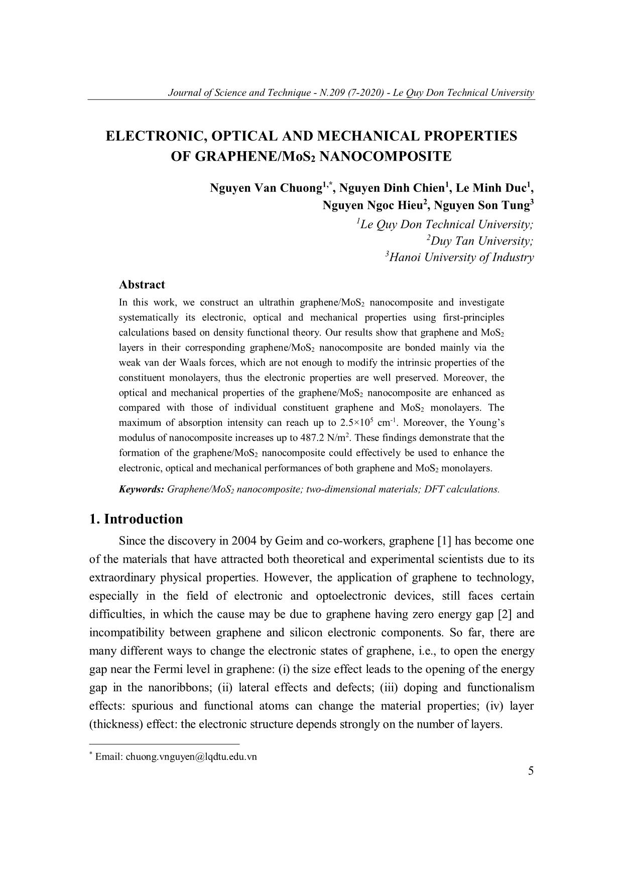
In this work, we construct an ultrathin graphene/MoS2 nanocomposite and investigate
systematically its electronic, optical and mechanical properties using first-principles
calculations based on density functional theory. Our results show that graphene and MoS2
layers in their corresponding graphene/MoS2 nanocomposite are bonded mainly via the
weak van der Waals forces, which are not enough to modify the intrinsic properties of the
constituent monolayers, thus the electronic properties are well preserved. Moreover, the
optical and mechanical properties of the graphene/MoS2 nanocomposite are enhanced as
compared with those of individual constituent graphene and MoS2 monolayers. The
maximum of absorption intensity can reach up to 2.5×105 cm-1. Moreover, the Young’s
modulus of nanocomposite increases up to 487.2 N/m2. These findings demonstrate that the
formation of the graphene/MoS2 nanocomposite could effectively be used to enhance the
electronic, optical and mechanical performances of both graphene and MoS2 monolayers
Trang 1
Trang 2
Trang 3
Trang 4
Trang 5
Trang 6
Trang 7
Trang 8
Trang 9
Trang 10
Tải về để xem bản đầy đủ
Tóm tắt nội dung tài liệu: Electronic, optical and mechanical properties of graphene/MoS₂ nanocomposite

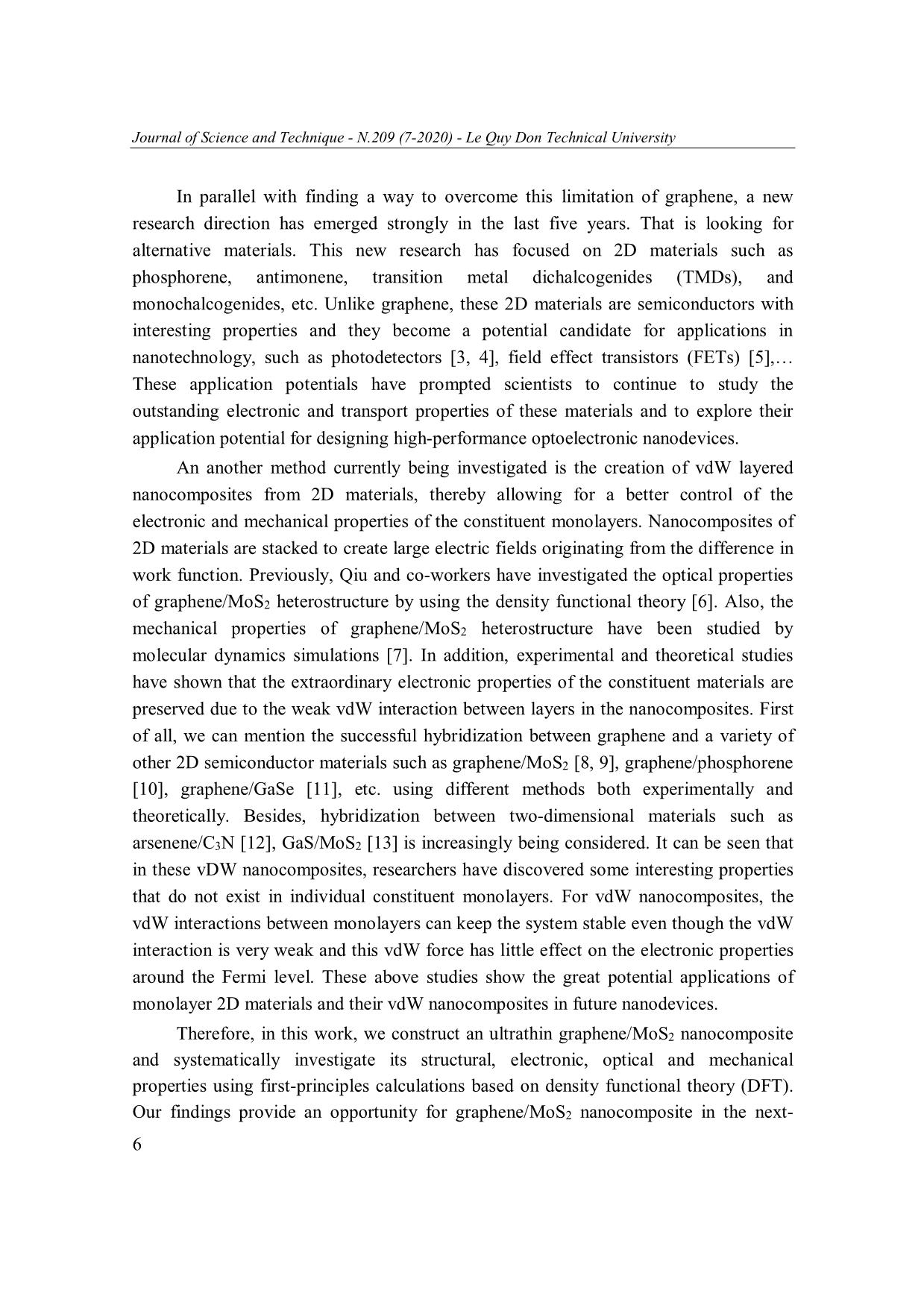
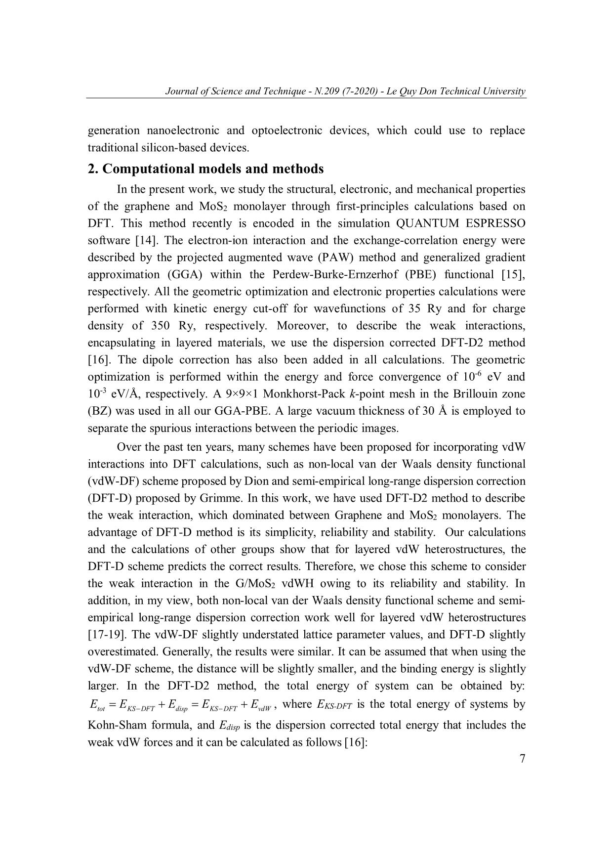
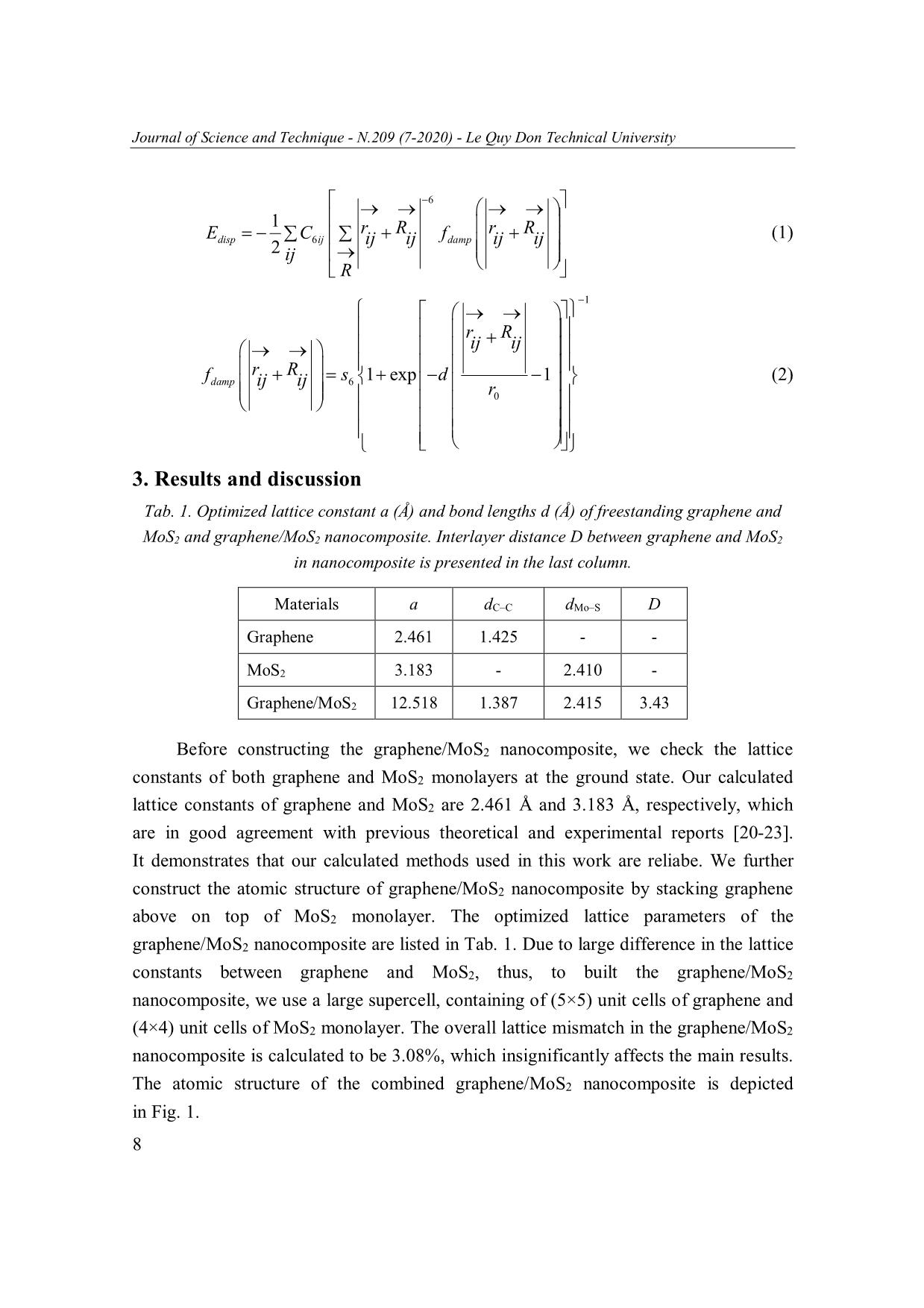
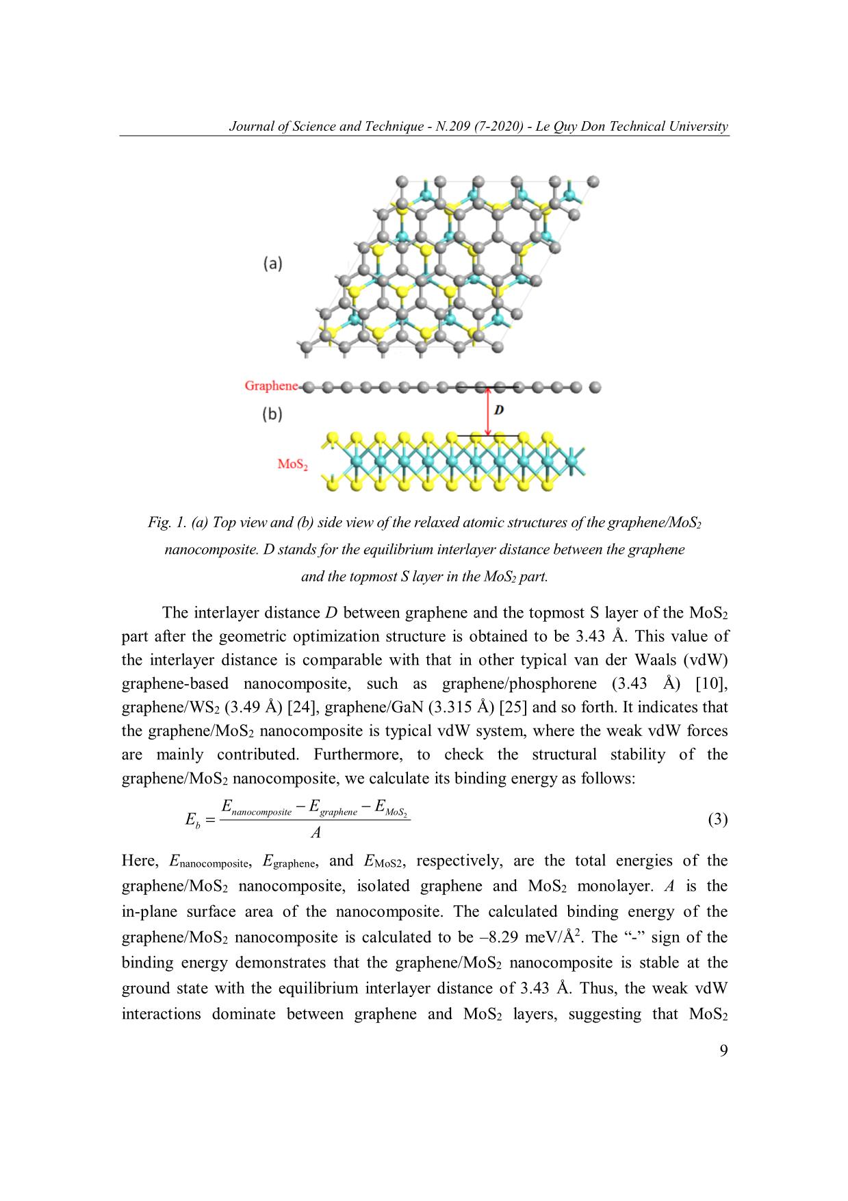
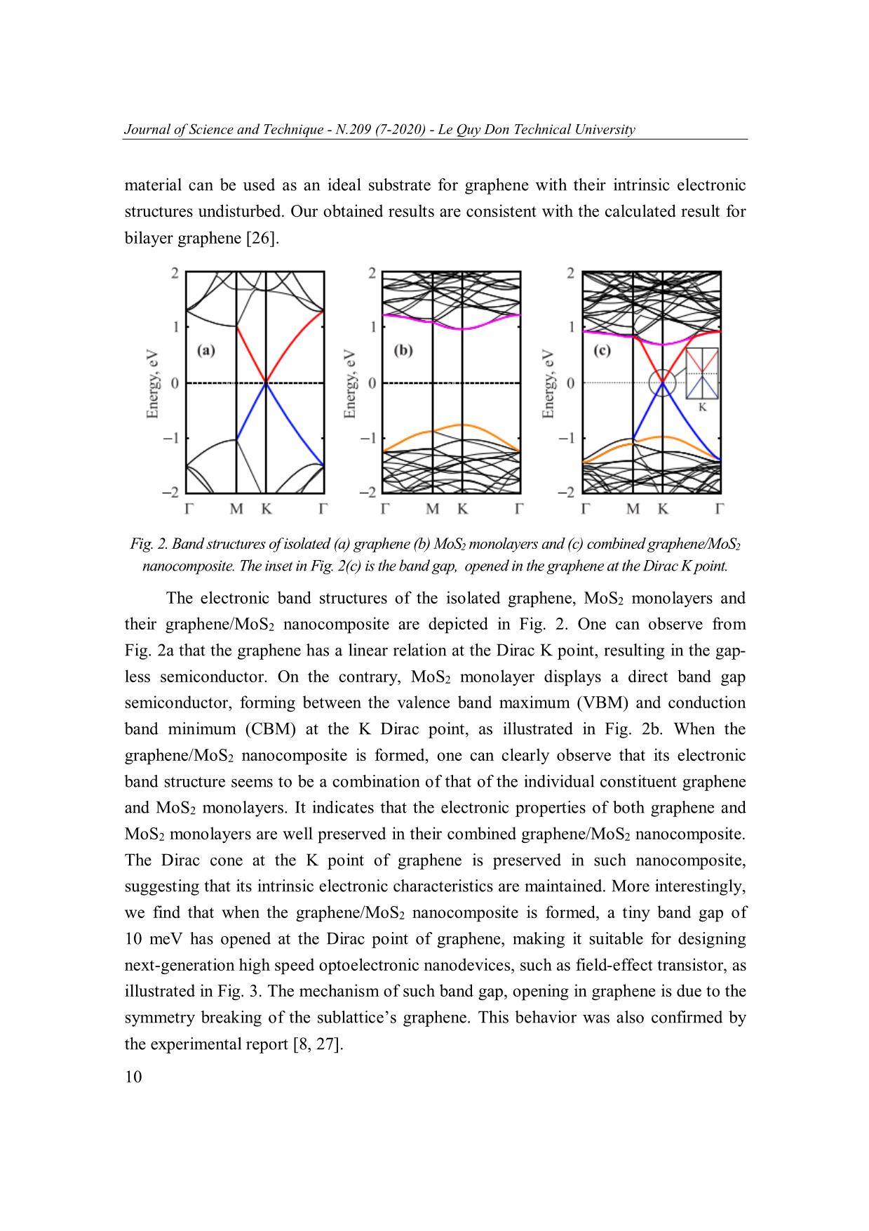
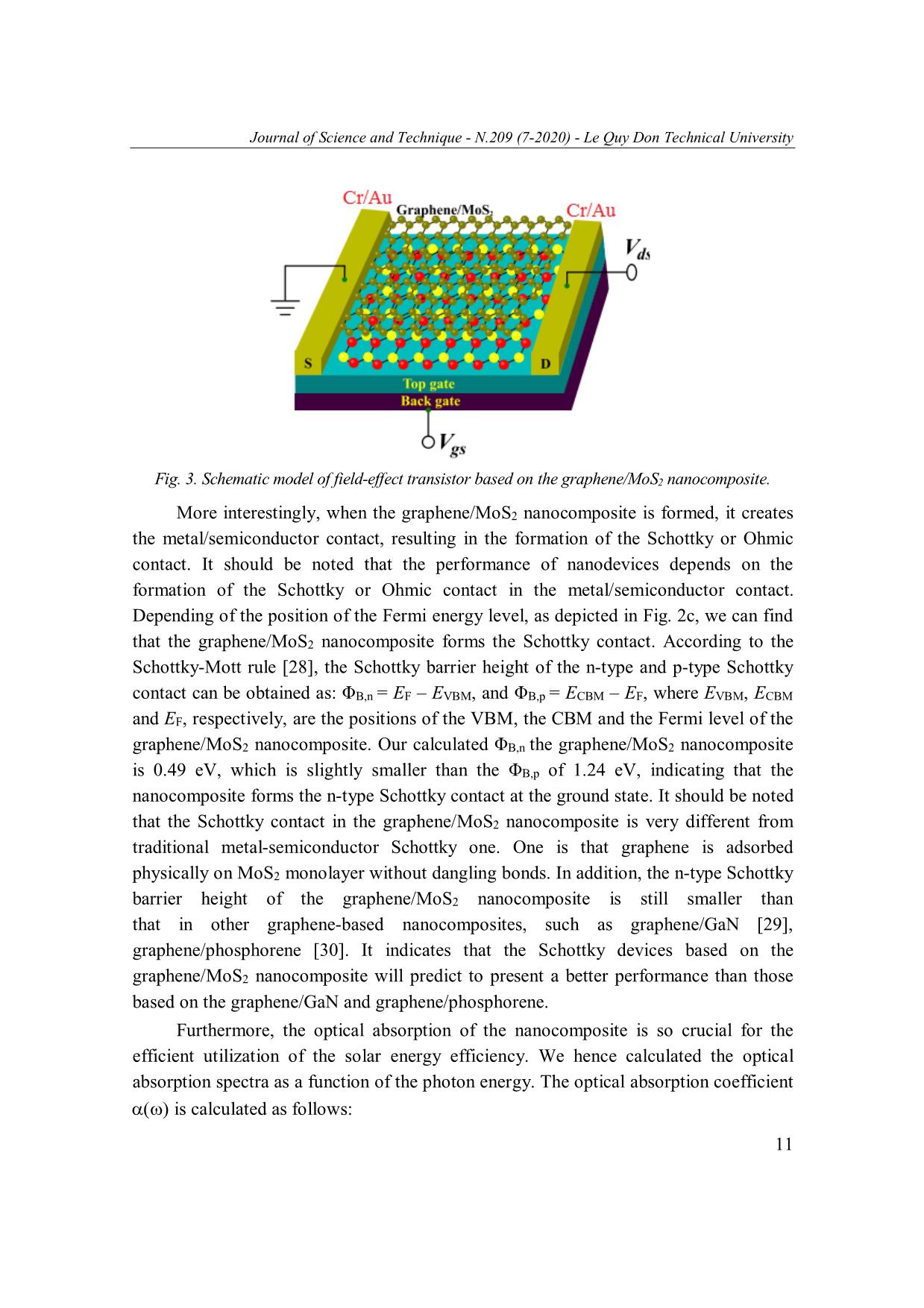
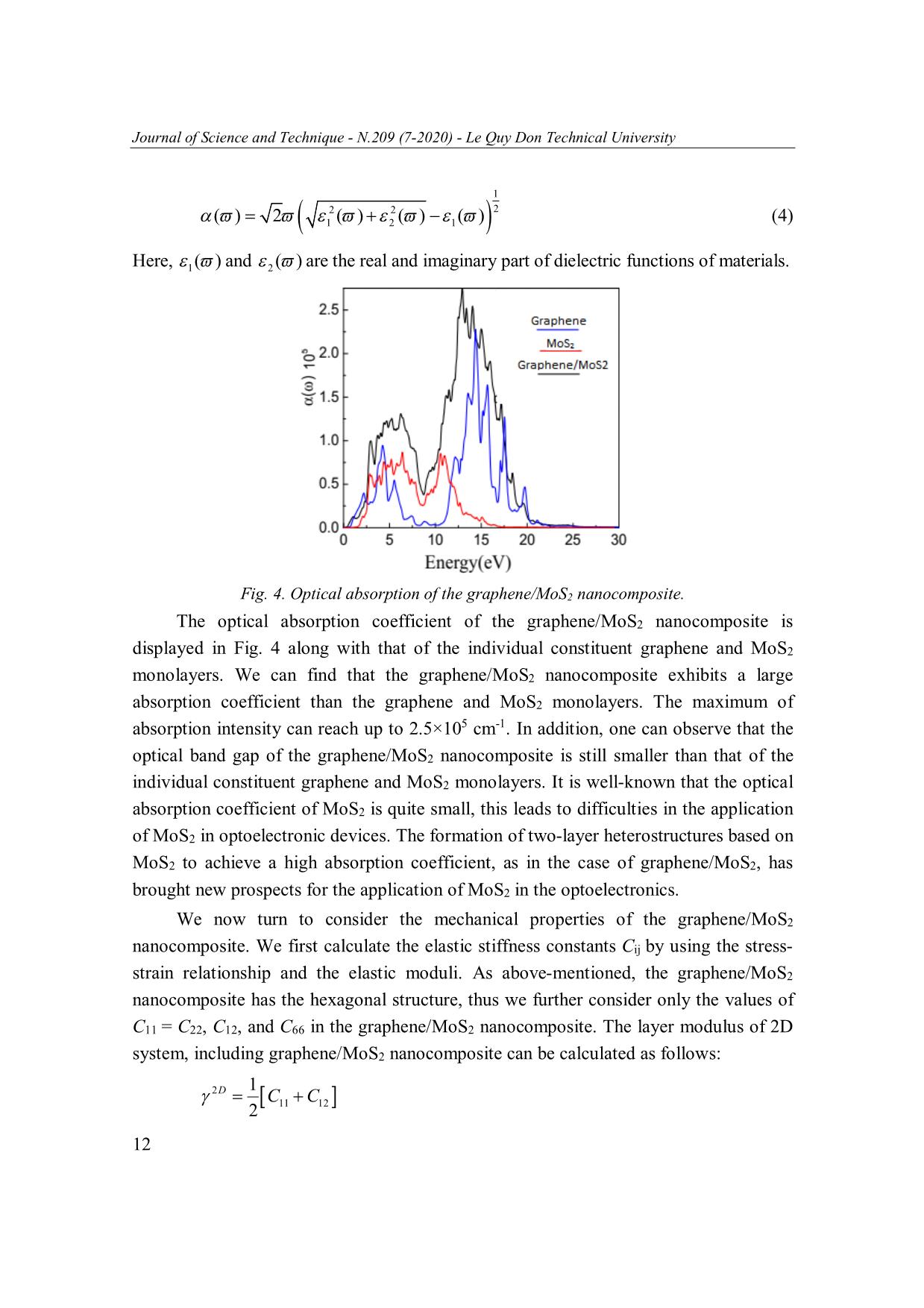
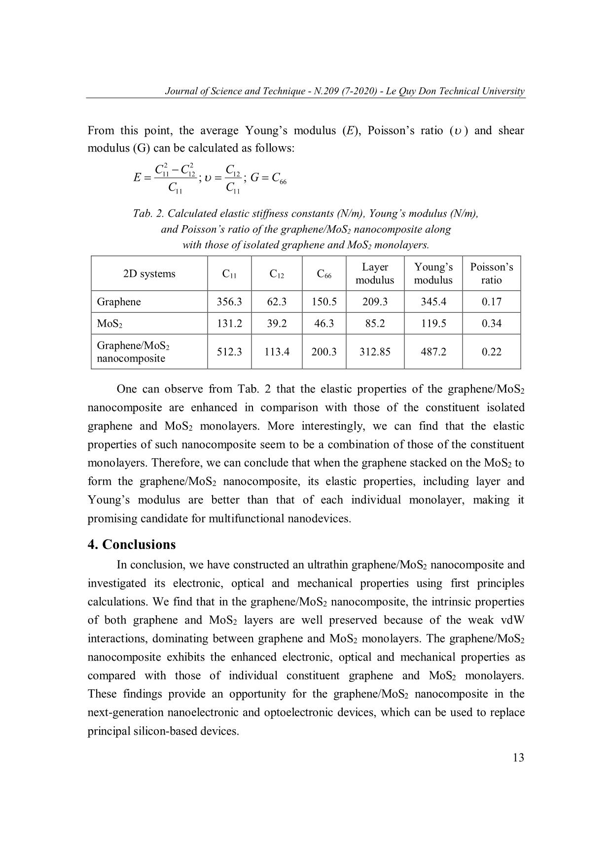
Journal of Science and Technique - N.209 (7-2020) - Le Quy Don Technical University ELECTRONIC, OPTICAL AND MECHANICAL PROPERTIES OF GRAPHENE/MoS2 NANOCOMPOSITE Nguyen Van Chuong1,*, Nguyen Dinh Chien1, Le Minh Duc1, Nguyen Ngoc Hieu2, Nguyen Son Tung3 1Le Quy Don Technical University; 2Duy Tan University; 3Hanoi University of Industry Abstract In this work, we construct an ultrathin graphene/MoS2 nanocomposite and investigate systematically its electronic, optical and mechanical properties using first-principles calculations based on density functional theory. Our results show that graphene and MoS2 layers in their corresponding graphene/MoS2 nanocomposite are bonded mainly via the weak van der Waals forces, which are not enough to modify the intrinsic properties of the constituent monolayers, thus the electronic properties are well preserved. Moreover, the optical and mechanical properties of the graphene/MoS2 nanocomposite are enhanced as compared with those of individual constituent graphene and MoS2 monolayers. The maximum of absorption intensity can reach up to 2.5×105 cm-1. Moreover, the Young’s modulus of nanocomposite increases up to 487.2 N/m2. These findings demonstrate that the formation of the graphene/MoS2 nanocomposite could effectively be used to enhance the electronic, optical and mechanical performances of both graphene and MoS2 monolayers. Keywords: Graphene/MoS2 nanocomposite; two-dimensional materials; DFT calculations. 1. Introduction Since the discovery in 2004 by Geim and co-workers, graphene [1] has become one of the materials that have attracted both theoretical and experimental scientists due to its extraordinary physical properties. However, the application of graphene to technology, especially in the field of electronic and optoelectronic devices, still faces certain difficulties, in which the cause may be due to graphene having zero energy gap [2] and incompatibility between graphene and silicon electronic components. So far, there are many different ways to change the electronic states of graphene, i.e., to open the energy gap near the Fermi level in graphene: (i) the size effect leads to the opening of the energy gap in the nanoribbons; (ii) lateral effects and defects; (iii) doping and functionalism effects: spurious and functional atoms can change the material properties; (iv) layer (thickness) effect: the electronic structure depends strongly on the number of layers. * Email: chuong.vnguyen@lqdtu.edu.vn 5 Journal of Science and Technique - N.209 (7-2020) - Le Quy Don Technical University In parallel with finding a way to overcome this limitation of graphene, a new research direction has emerged strongly in the last five years. That is looking for alternative materials. This new research has focused on 2D materials such as phosphorene, antimonene, transition metal dichalcogenides (TMDs), and monochalcogenides, etc. Unlike graphene, these 2D materials are semiconductors with interesting properties and they become a potential candidate for applications in nanotechnology, such as photodetectors [3, 4], field effect transistors (FETs) [5], These application potentials have prompted scientists to continue to study the outstanding electronic and transport properties of these materials and to explore their application potential for designing high-performance optoelectronic nanodevices. An another method currently being investigated is the creation of vdW layered nanocomposites from 2D materials, thereby allowing for a better control of the electronic and mechanical properties of the constituent monolayers. Nanocomposites of 2D materials are stacked to create large electric fields originating from the difference in work function. Previously, Qiu and co-workers have investigated the optical properties of graphene/MoS2 heterostructure by using the density functional theory [6]. Also, the mechanical properties of graphene/MoS2 heterostructure have been studied by molecular dynamics simulations [7]. In addition, experimental and theoretical studies have shown that the extraordinary electronic properties of the constituent materials are preserved due to the weak vdW interaction between layers in the nanocomposites. First of all, we can mention the successful hybridization between graphene and a variety of other 2D semiconductor materials such as graphene/MoS2 [8, 9], graphene/phosphorene [10], graphene/GaSe [11], etc. using different methods both experimentally and theoretically. Besides, hybridization between two-dimensional materials such as arsenene/C3N [12], GaS/MoS2 [13] is increasingly being considered. It can be seen that in these vDW nanocomposites, researchers have discovered some interesting properties that do not exist in individual constituent monolayers. For vdW nanocomposites, the vdW interactions between monolayers can ke ... of the isolated graphene, MoS2 monolayers and their graphene/MoS2 nanocomposite are depicted in Fig. 2. One can observe from Fig. 2a that the graphene has a linear relation at the Dirac K point, resulting in the gap- less semiconductor. On the contrary, MoS2 monolayer displays a direct band gap semiconductor, forming between the valence band maximum (VBM) and conduction band minimum (CBM) at the K Dirac point, as illustrated in Fig. 2b. When the graphene/MoS2 nanocomposite is formed, one can clearly observe that its electronic band structure seems to be a combination of that of the individual constituent graphene and MoS2 monolayers. It indicates that the electronic properties of both graphene and MoS2 monolayers are well preserved in their combined graphene/MoS2 nanocomposite. The Dirac cone at the K point of graphene is preserved in such nanocomposite, suggesting that its intrinsic electronic characteristics are maintained. More interestingly, we find that when the graphene/MoS2 nanocomposite is formed, a tiny band gap of 10 meV has opened at the Dirac point of graphene, making it suitable for designing next-generation high speed optoelectronic nanodevices, such as field-effect transistor, as illustrated in Fig. 3. The mechanism of such band gap, opening in graphene is due to the symmetry breaking of the sublattice’s graphene. This behavior was also confirmed by the experimental report [8, 27]. 10 Journal of Science and Technique - N.209 (7-2020) - Le Quy Don Technical University Fig. 3. Schematic model of field-effect transistor based on the graphene/MoS2 nanocomposite. More interestingly, when the graphene/MoS2 nanocomposite is formed, it creates the metal/semiconductor contact, resulting in the formation of the Schottky or Ohmic contact. It should be noted that the performance of nanodevices depends on the formation of the Schottky or Ohmic contact in the metal/semiconductor contact. Depending of the position of the Fermi energy level, as depicted in Fig. 2c, we can find that the graphene/MoS2 nanocomposite forms the Schottky contact. According to the Schottky-Mott rule [28], the Schottky barrier height of the n-type and p-type Schottky contact can be obtained as: ΦB,n = EF – EVBM, and ΦB,p = ECBM – EF, where EVBM, ECBM and EF, respectively, are the positions of the VBM, the CBM and the Fermi level of the graphene/MoS2 nanocomposite. Our calculated ΦB,n the graphene/MoS2 nanocomposite is 0.49 eV, which is slightly smaller than the ΦB,p of 1.24 eV, indicating that the nanocomposite forms the n-type Schottky contact at the ground state. It should be noted that the Schottky contact in the graphene/MoS2 nanocomposite is very different from traditional metal-semiconductor Schottky one. One is that graphene is adsorbed physically on MoS2 monolayer without dangling bonds. In addition, the n-type Schottky barrier height of the graphene/MoS2 nanocomposite is still smaller than that in other graphene-based nanocomposites, such as graphene/GaN [29], graphene/phosphorene [30]. It indicates that the Schottky devices based on the graphene/MoS2 nanocomposite will predict to present a better performance than those based on the graphene/GaN and graphene/phosphorene. Furthermore, the optical absorption of the nanocomposite is so crucial for the efficient utilization of the solar energy efficiency. We hence calculated the optical absorption spectra as a function of the photon energy. The optical absorption coefficient is calculated as follows: 11 Journal of Science and Technique - N.209 (7-2020) - Le Quy Don Technical University 1 ( ) 2 2 ( ) 2 ( ) ( ) 2 (4) 1 2 1 Here, 1() and 2 () are the real and imaginary part of dielectric functions of materials. Fig. 4. Optical absorption of the graphene/MoS2 nanocomposite. The optical absorption coefficient of the graphene/MoS2 nanocomposite is displayed in Fig. 4 along with that of the individual constituent graphene and MoS2 monolayers. We can find that the graphene/MoS2 nanocomposite exhibits a large absorption coefficient than the graphene and MoS2 monolayers. The maximum of absorption intensity can reach up to 2.5×105 cm-1. In addition, one can observe that the optical band gap of the graphene/MoS2 nanocomposite is still smaller than that of the individual constituent graphene and MoS2 monolayers. It is well-known that the optical absorption coefficient of MoS2 is quite small, this leads to difficulties in the application of MoS2 in optoelectronic devices. The formation of two-layer heterostructures based on MoS2 to achieve a high absorption coefficient, as in the case of graphene/MoS2, has brought new prospects for the application of MoS2 in the optoelectronics. We now turn to consider the mechanical properties of the graphene/MoS2 nanocomposite. We first calculate the elastic stiffness constants Cij by using the stress- strain relationship and the elastic moduli. As above-mentioned, the graphene/MoS2 nanocomposite has the hexagonal structure, thus we further consider only the values of C11 = C22, C12, and C66 in the graphene/MoS2 nanocomposite. The layer modulus of 2D system, including graphene/MoS2 nanocomposite can be calculated as follows: 1 2D CC 2 11 12 12 Journal of Science and Technique - N.209 (7-2020) - Le Quy Don Technical University From this point, the average Young’s modulus (E), Poisson’s ratio ( ) and shear modulus (G) can be calculated as follows: 2 2 CCC11 12 12 EGC ;; 66 CC11 11 Tab. 2. Calculated elastic stiffness constants (N/m), Young’s modulus (N/m), and Poisson’s ratio of the graphene/MoS2 nanocomposite along with those of isolated graphene and MoS2 monolayers. Layer Young’s Poisson’s 2D systems C C C 11 12 66 modulus modulus ratio Graphene 356.3 62.3 150.5 209.3 345.4 0.17 MoS2 131.2 39.2 46.3 85.2 119.5 0.34 Graphene/MoS 2 512.3 113.4 200.3 312.85 487.2 0.22 nanocomposite One can observe from Tab. 2 that the elastic properties of the graphene/MoS2 nanocomposite are enhanced in comparison with those of the constituent isolated graphene and MoS2 monolayers. More interestingly, we can find that the elastic properties of such nanocomposite seem to be a combination of those of the constituent monolayers. Therefore, we can conclude that when the graphene stacked on the MoS2 to form the graphene/MoS2 nanocomposite, its elastic properties, including layer and Young’s modulus are better than that of each individual monolayer, making it promising candidate for multifunctional nanodevices. 4. Conclusions In conclusion, we have constructed an ultrathin graphene/MoS2 nanocomposite and investigated its electronic, optical and mechanical properties using first principles calculations. We find that in the graphene/MoS2 nanocomposite, the intrinsic properties of both graphene and MoS2 layers are well preserved because of the weak vdW interactions, dominating between graphene and MoS2 monolayers. The graphene/MoS2 nanocomposite exhibits the enhanced electronic, optical and mechanical properties as compared with those of individual constituent graphene and MoS2 monolayers. These findings provide an opportunity for the graphene/MoS2 nanocomposite in the next-generation nanoelectronic and optoelectronic devices, which can be used to replace principal silicon-based devices. 13 Journal of Science and Technique - N.209 (7-2020) - Le Quy Don Technical University Acknowledgements This research is funded by the Vietnam National Foundation for Science and Technology Development (NAFOSTED) under grant number 103.01-2019.05. References 1. K. S. Novoselov, A. K. Geim, S. V. Morozov, D. Jiang, Y. Zhang, S. V. Dubonos, I. V. Grigorieva, and A. A. Firsov (2004). Electric field effect in atomically thin carbon films. Science, 306, 666-669. 2. K. S. Novoselov, A. K. Geim, S. Morozov, D. Jiang, M. I. Katsnelson, I. Grigorieva, S. Dubonos, Firsov, and A. A. Firsov (2005). Two-dimensional gas of massless Dirac fermions in graphene. Nature, 438, 197. 3. F. Koppens, T. Mueller, P. Avouris, A. Ferrari, M. Vitiello, and M. Polini (2014). Photodetectors based on graphene, other two-dimensional materials and hybrid systems, Nature Nanotechnology, 9, 780. 4. C. Xie, C. Mak, X. Tao, and F. Yan (2017). Photodetectors based on two‐dimensional layered materials beyond graphene. Advanced Functional Materials, 27, 1603886. 5. L. Li, Y. Yu, G. J. Ye, Q. Ge, X. Ou, H. Wu, D. Feng, X. H. Chen, and Y. Zhang (2014). Black phosphorus field-effect transistors. Nature Nanotechnology, 9, 372. 6. B. Qiu, X. Zhao, G. Hu, W. Yue, J. Ren, and X. Yuan (2018). Optical Properties of Graphene/MoS2 Heterostructure: First Principles Calculations. Nanomaterials, 8, 962. 7. J.-W. Jiang and H. S. Park (2014). Mechanical properties of MoS2/graphene heterostructures. Applied Physics Letters, 105, 033108. 8. Z. B. Aziza, H. Henck, D. Di Felice, D. Pierucci, J. Chaste, C. H. Naylor, A. Balan, Y. J. Dappe, A. C. Johnson, and A. Ouerghi (2016). Bandgap inhomogeneity of MoS2 monolayer on epitaxial graphene bilayer in van der Waals p-n junction. Carbon, 110, 396-403. 9. N. N. Hieu, H. V. Phuc, V. V. Ilyasov, N. D. Chien, N. A. Poklonski, N. Van Hieu, and C. V. Nguyen (2017). First-principles study of the structural and electronic properties of graphene/MoS2 interfaces. Journal of Applied Physics, 122, 104301. 10. W. Hu, T. Wang, and J. Yang (2015). Tunable Schottky contacts in hybrid graphene– phosphorene nanocomposites. Journal of Materials Chemistry C, 3, 4756-4761. 11. R. Lu, J. Liu, H. Luo, V. Chikan, and J. Z. Wu (2016). Graphene/GaSe-nanosheet hybrid: Towards high gain and fast photoresponse. Scientific Reports, 6, 19161. 12. H. Zeng, J. Zhao, A.-Q. Cheng, L. Zhang, Z. He, and R.-S. Chen (2018). Tuning electronic and optical properties of arsenene/C3N van der Waals heterostructure by vertical strain and external electric field. Nanotechnology, 29, 075201. 13. Q. Zhang and U. Schwingenschlögl (2018). Rashba effect and enriched spin-valley coupling in Ga X/MX2 (M = Mo, W; X = S, Se, Te) heterostructures. Physical Review B, 97, 155415. 14 Journal of Science and Technique - N.209 (7-2020) - Le Quy Don Technical University 14. P. Giannozzi, S. Baroni, N. Bonini, M. Calandra, R. Car, C. Cavazzoni, D. Ceresoli, G. L. Chiarotti, M. Cococcioni, and I. Dabo (2009). QUANTUM ESPRESSO: A modular and open-source software project for quantum simulations of materials. Journal of Physics: Condensed Matter, 21, 395502. 15. J. P. Perdew, K. Burke, and M. Ernzerhof (1996). Generalized gradient approximation made simple. Physical Review Letters, 77, 3865. 16. S. Grimme (2006). Semiempirical GGA‐type density functional constructed with a long‐range dispersion correction. Journal of Computational Chemistry, 27, 1787-1799. 17. I. V. Lebedeva, A. V. Lebedev, A. M. Popov, and A. A. Knizhnik (2017). Comparison of performance of van der Waals-corrected exchange-correlation functionals for interlayer interaction in graphene and hexagonal boron nitride. Computational Materials Science, 128, 45-58. 18. S. A. Tawfik, T. Gould, C. Stampfl, and M. J. Ford (2018). Evaluation of van der Waals density functionals for layered materials. Physical Review Materials, 2, 034005. 19. T. Björkman, A. Gulans, A. Krasheninnikov, and R. Nieminen (2012). Are we van der Waals ready? Journal of Physics: Condensed Matter, 24, 424218. 20. A. K. Geim and K. S. Novoselov (2007). The rise of graphene. Nature Materials, 6, 183-191. 21. J. A. Wilson and A. Yoffe (1969). The transition metal dichalcogenides discussion and interpretation of the observed optical, electrical and structural properties. Advances in Physics, 18, 193-335. 22. P. Johari and V. B. Shenoy (2012). Tuning the electronic properties of semiconducting transition metal dichalcogenides by applying mechanical strains. ACS nano, 6, 5449-5456. 23. A. C. Neto, F. Guinea, N. M. Peres, K.S. Novoselov, and A. K. Geim (2009). The electronic properties of graphene. Reviews of Modern Physics, 81, 109. 24. F. Zhang, W. Li, Y. Ma, Y. Tang, and X. Dai (2017). Tuning the Schottky contacts at the graphene/WS2 interface by electric field. RSC Advances, 7, 29350-29356. 25. Z. Deng and X. Wang (2019). Strain engineering on the electronic states of two- dimensional GaN/graphene heterostructure. RSC Advances, 9, 26024-26029. 26. E. Mostaani, N. Drummond, and V. Fal’Ko (2015). Quantum Monte Carlo calculation of the binding energy of bilayer graphene. Physical Review Letters, 115, 115501. 27. D. Pierucci, H. Henck, J. Avila, A. Balan, C. H. Naylor, G. Patriarche, Y. J. Dappe, M. G. Silly, F. Sirotti, and A. C. Johnson (2016). Band alignment and minigaps in monolayer MoS2-graphene van der Waals heterostructures. Nano Letters, 16, 4054-4061. 28. J. Bardeen (1947). Surface states and rectification at a metal semi-conductor contact. Physical Review, 71, 717. 29. M. Sun, J.-P. Chou, Q. Ren, Y. Zhao, J. Yu, and W. Tang (2017). Tunable Schottky barrier in van der Waals heterostructures of graphene and g-GaN. Applied Physics Letters, 110, 173105. 30. B. Liu, L.-J. Wu, Y.-Q. Zhao, L.-Z. Wang, and M.-Q. Caii (2016). Tuning the Schottky contacts in the phosphorene and graphene heterostructure by applying strain. Physical Chemistry Chemical Physics, 18, 19918-19925. 15 Journal of Science and Technique - N.209 (7-2020) - Le Quy Don Technical University NGHIÊN CỨU CÁC TÍNH CHẤT ĐIỆN TỬ, QUANG HỌC VÀ CƠ TÍNH CỦA VẬT LIỆU NANO COMPOSITE GRAPHENE/MoS2 Tóm tắt: Trong bài báo này, chúng tôi mô phỏng và nghiên cứu các tính chất điện tử, quang học và cơ tính của hệ vật liệu màng mỏng nano graphene/MoS2 sử dụng lý thuyết phiếm hàm mật độ. Kết quả nghiên cứu cho thấy lực tương tác yếu van der Waals giữa các lớp vật liệu giữ cho hệ vật liệu nanocomposite graphene/MoS2 bền vững và không gây phá hủy các tính chất điện tử nổi trội của graphene và MoS2 đơn lớp. Bên cạnh đó, chúng tôi thấy rằng các tính chất quang học và cơ tính của graphene và MoS2 được tăng cường trong hệ vật liệu nanocomposite. Hệ số quang hấp thụ tối đa của hệ có thể đạt 2,5×105 cm-1. Trong khi đó, mô đun đàn hồi Young của hệ nanocomposite này tăng lên tới 487,2 N/m2. Các kết quả nghiên cứu này chỉ ra rằng sự hình thành hệ vật liệu màng mỏng nanocomposite của graphene và MoS2 là phương pháp hiệu dụng để tăng cường các tính chất điện tử, quang học cũng như cơ tính của các vật liệu tiềm năng graphene và MoS2. Từ khóa: Vật liệu nanocomposite graphene/MoS2; các vật liệu hai chiều; phương pháp phiếm hàm mật độ. Received: 10/02/2020; Revised: 26/7/2020; Accepted for publication: 28/7/2020 16
File đính kèm:
 electronic_optical_and_mechanical_properties_of_graphenemos.pdf

